Making synthetic diamond crystals in a plasma reactor
Direktzugriff
Artikelaktionen
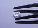
A high-purity single-crystal diamond made at Fraunhofer IAF.
Diamonds are highly sought after as jewelry and as a form of capital investment. They are also prized by the research community, but not because of their brilliance or symbolic significance – it is their physical properties that make these gems precious to scientists. Diamonds are extremely hard, have unrivaled thermal conductivity and have a broadband spectral transparency that stretches from ultraviolet to far infrared, making them the ideal material for a host of different applications. Consequently, there is a large market for synthetic diamonds: they can cut through steel as if it were paper, dig their way through the earth on the tips of drilling heads, are used as scalpels in operations and can act as bio-electrochemical sensors for detecting substances such as DNA.
Researchers at the Fraunhofer Institute for Applied Solid State Physics IAF in Freiburg make synthetic diamonds of the highest quality. They produce three-dimensional geometries and discs of different diameters and thicknesses using plasma-enhanced chemical vapor deposition (CVD), a process by which diamond is chemically deposited on a substrate from the gas phase. A specially pretreated silicon or silicon dioxide (silica) substrate is coated with diamond by means of microwave plasma in an ellipsoidal reactor. Fraunhofer IAF’s diamond laboratory contains eight such plasma reactors for growing diamonds in polycrystalline (that is, made up of countless smaller crystals) and single-crystal form. Scientists can determine the orientation of polycrystalline diamond growth by applying small diamond seed crystals to the substrate before plasma deposition occurs. Single-crystalline diamonds with a continuous homogenous crystal lattice structure, however, have to be grown on a single-crystal diamond substrate. “We use chemical vapour deposition because it allows us to coat larger substrates, unlike other manufacturing processes such as the high pressure high temperature method. What’s more, this method will enable us to produce diamonds of high enough quality for use in electronic applications, and means we can homogeneously deposit diamonds with diameters of up to 10 cm on silicon substrates,” states Nicola Heidrich, group manager at Fraunhofer IAF. But making diamonds requires patience: a 100-nanometer-thick poly- or nanocrystalline layer can be grown within an hour; single crystals grow at a rate of up to 20 micrometers an hour.
Electronic sniffer devices detect impurities
One of the advantages of single crystals is their reproducible properties. They are worked into regular geometric shapes and used for applications in the optical and electronic fields, among others. Optical applications are also an area that polycrystalline diamonds are suited to thanks to their mechanical stability and transparency over a very broad spectral range. At Fraunhofer IAF the material is used to fabricate form-flexible micro lenses. The lens is shaped using positive air pressure, which bends the membrane and gives it a curved shape. Increasing the pressure allows scientists to increase the curvature and thus set the focal distance of the diamond membrane. Since diamond is chemically resistant, bio-compatible and able to withstand extreme temperatures, scientists are using it to develop electrochemical sensors that will in the future enable them to monitor water quality over long periods of time. Diamond is also an electrical insulator that can be turned into a conductor by adding boron and phosphorous to it. Researchers are working on ways to exploit its outstanding electronic properties for use in the high-performance transistors and components based on quantum effects of the future.
Diamond spheres for tomorrow’s energy
Fraunhofer IAF experts have mastered the art of producing tiny hollow spheres of synthetic diamond in partnership with Diamond Materials GmbH, a Fraunhofer spin-off based in Freiburg. These little balls could play a central part in future energy production by means of atomic fusion. American scientists are constructing a nuclear fusion reactor in order to tap a source of energy modeled on the sun. The nuclear reaction is triggered when laser beams impact a hollow hydrogen-filled sphere 2 mm in diameter and compresses it to about one ten-thousandth of its original volume. This process fuses the atomic nuclei, releasing enormous amounts of energy. However, for the fusion process to work the balls must be perfectly spherical and have no structural flaws – only then can the huge forces achieve the calculated fusion requirements. “Diamond has the ideal properties for this application,” says Heidrich. But how do they make flat discs into balls? At the core of the solution are tiny silicon globules that are kept constantly in motion in a plasma reactor as they are coated with diamond. It takes about 50 hours for the desired thickness of diamond to build up, at which point the scientists polish the spheres and remove the silicon from inside. To get it out, they drill a tiny hole and then dissolve the silicon out of the ball using a special etching technique based on ultrasound. The hole later serves as the entry point through which they feed the deuterium and tritium fusion charge into the ball.
Fußzeile
Benutzerspezifische Werkzeuge

