Soft Probing with Optical Tweezers
Direktzugriff
Artikelaktionen
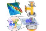
A laser trapping beam (orange) moves the probe (green sphere) over the structured surface (blue spheres), where the beam is displaced depending on the height of the structure. Image: Rohrbach group.
Surfaces separate outside from inside, control chemical reactions, and regulate the exchange of light, heat, and moisture. They thus play a special role in nature and technology. In the journal Nature Nanotechnology, the Freiburg physicist Prof. Dr. Alexander Rohrbach and his former PhD candidate Dr. Lars Friedrich have presented an ultra-soft surface scanning method based on an optical trap and optical forces. Microscopy methods like these make it possible to measure particularly sensitive and minuscule structures without destroying them.
The measuring apparatus is based on a so-called photonic force microscope (PFM) and has the purpose of generating height profiles of soft surfaces like biofilms or cell membranes. It probes a sample up to 5000 times more gently and sensitively than the atomic force microscope (AFM), which is well-established in nanotechnology. An AFM uses a small spring arm – a needle with an ultra-thin tip – to scan a surface. The microscope measures the speed at which the tip moves and uses this information to create a two-dimensional surface profile. In a PFM, the spring arm is replaced by a small plastic sphere that sits at the center of a so-called optical trap and runs along the surface. An optical trap is created by a highly focused laser beam and can be used to hold or move miniscule objects. The sphere is less than 200 nanometers in diameter, making it 500 times thinner than a human hair. The PFM also measures changes in surface height, which displace the sphere from its course, creating a height profile point by point in this way. Although a PFM is not capable of imaging such fine structures as an AFM, it exerts less pressure on the surface, for instance that of a cell, and thus does not deform it. “The basic idea for this technique is actually almost 20 years old,” explains Alexander Rohrbach, “but we had to solve a lot of conceptual problems before we could present a practicable and dependable measurement system.”
Rohrbach and Friedrich made use of mechanisms that measurement engineers usually try to avoid: scattered light and thermal noise. The tiny plastic sphere, the probe, appears to move in a chaotic manner inside the light trap due to the so-called thermal noise. The optical trap moves the probe along the structured surface, where the probe is displaced depending on the height of the structure. This displacement is detected by the laser beam scattered at the probe. In this way, the three-dimensional position of the probe is measured one million times per second. “The most remarkable thing is that the quivering probe is repeatedly left alone briefly so that the laser beam can jump a step forward for a millisecond,” explains Rohrbach. “Once there, the probe records the scattered light from the surface and subtracts it. But before the probe can escape, the laser beam has trapped it again.”
Among other things, the Freiburg researchers have used their technique to scan bacteria, which have tiny protrusions on their surface. These so-called pili probably play a role in the communication between bacteria. They react to the softest amount of pressure, and this makes the new technology especially suited to studying them. “In the coming years, we want to scan other and different surfaces by adopting and adapting several measurement principles from the AFM technology,” says Rohrbach.
Alexander Rohrbach conducts research at the Department of Microsystems Engineering (IMTEK) and is an associate member of the Cluster of Excellence BIOSS Centre for Biological Signalling Studies of the University of Freiburg.
Original publication:
Lars Friedrich, Alexander Rohrbach (2015). Surface imaging beyond the diffraction limit with optically trapped spheres. In: Nature Nanotechnology. doi:10.1038/nnano.2015.202
Contact:
Prof. Dr. Alexander Rohrbach
Department of Microsystems Engineering
University of Freiburg
Phone: +49 (0)761/203-7536
E-Mail: rohrbach(at)imtek.uni-freiburg.de
Printable version (pdf) of the press release.
Fußzeile
Benutzerspezifische Werkzeuge

